- 您现在的位置:买卖IC网 > Sheet目录312 > AT26DF161-SU (Atmel)IC FLASH 16MBIT 66MHZ 8SOIC
AT26DF161
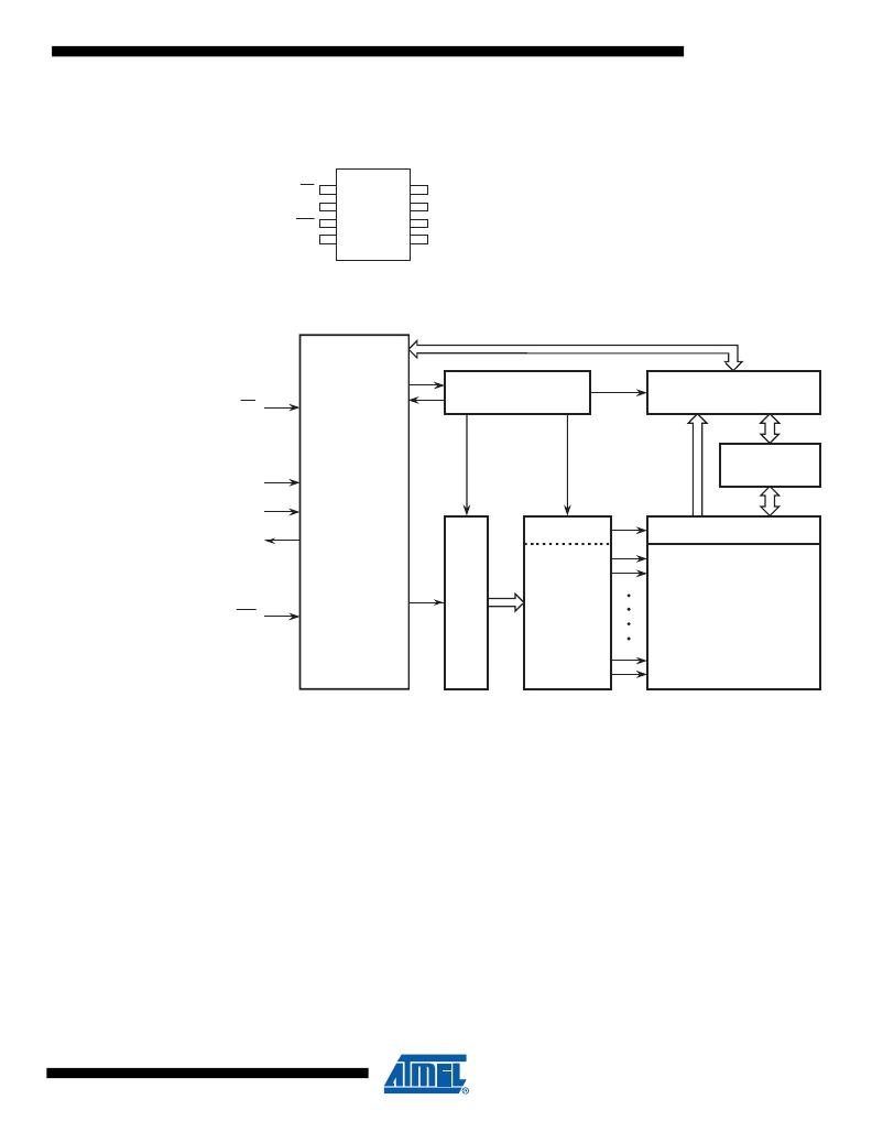
Figure 2-1.
8-SOIC Top View
CS
SO
WP
GND
1
2
3
4
8
7
6
5
VCC
NC
SCK
SI
3. Block Diagram
CONTROL AND
I/O BUFFERS
CS
SCK
INTERFACE
PROTECTION LOGIC
AND LATCHES
SRAM
DATA BUFFER
SI
SO
CONTROL
AND
LOGIC
Y-DECODER
Y-GATING
FLASH
WP
X-DECODER
MEMORY
ARRAY
4. Memory Array
To provide the greatest flexibility, the memory array of the AT26DF161 can be erased in four lev-
els of granularity including a full chip erase. In addition, the array has been divided into physical
sectors of uniform size, of which each sector can be individually protected from program and
erase operations. The size of the physical sectors is optimized for both code and data storage
applications, allowing both code and data segments to reside in their own isolated
regions. Figure 4-1 on page 4 illustrates the breakdown of each erase level as well as the break-
down of each physical sector.
3
3599H–DFLASH–8/09
发布紧急采购,3分钟左右您将得到回复。
相关PDF资料
AT26DF161A-MU
IC FLASH 16MBIT 70MHZ 8QFN
AT26DF321-SU
IC FLASH 32MBIT 66MHZ 8SOIC
AT27BV010-90JU
IC OTP 1MBIT 90NS 32PLCC
AT27BV020-90JU
IC OTP 2MBIT 90NS 32PLCC
AT27BV040-12JU
IC OTP 4MBIT 120NS 32PLCC
AT27BV1024-90JU
IC OTP 1MBIT 90NS 44PLCC
AT27BV256-70JU
IC OTP 256KBIT 70NS 32PLCC
AT27BV4096-12VI
IC OTP 4MBIT 120NS 40VSOP
相关代理商/技术参数
AT26DF321
制造商:ATMEL 制造商全称:ATMEL Corporation 功能描述:32-megabit 2.7-volt Only Serial Firmware DataFlash Memory
AT26DF321_06
制造商:ATMEL 制造商全称:ATMEL Corporation 功能描述:32-megabit 2.7-volt Only Serial Firmware DataFlash Memory
AT26DF321_07
制造商:ATMEL 制造商全称:ATMEL Corporation 功能描述:32-megabit 2.7-volt Only Serial Firmware DataFlash Memory
AT26DF321-S3U
功能描述:闪存 32M SERIAL FLASH - IND TEMP RoHS:否 制造商:ON Semiconductor 数据总线宽度:1 bit 存储类型:Flash 存储容量:2 MB 结构:256 K x 8 定时类型: 接口类型:SPI 访问时间: 电源电压-最大:3.6 V 电源电压-最小:2.3 V 最大工作电流:15 mA 工作温度:- 40 C to + 85 C 安装风格:SMD/SMT 封装 / 箱体: 封装:Reel
AT26DF321-SU
功能描述:闪存 32M SERIAL FLASH - IND TEMP RoHS:否 制造商:ON Semiconductor 数据总线宽度:1 bit 存储类型:Flash 存储容量:2 MB 结构:256 K x 8 定时类型: 接口类型:SPI 访问时间: 电源电压-最大:3.6 V 电源电压-最小:2.3 V 最大工作电流:15 mA 工作温度:- 40 C to + 85 C 安装风格:SMD/SMT 封装 / 箱体: 封装:Reel
AT26DF321-SU SL514
制造商:Atmel Corporation 功能描述:
AT26F004
制造商:ATMEL 制造商全称:ATMEL Corporation 功能描述:4-megabit 2.7-volt Only Serial Firmware DataFlash Memory
AT26F004_06
制造商:ATMEL 制造商全称:ATMEL Corporation 功能描述:4-megabit 2.7-volt Only Serial Firmware DataFlash Memory
